The basic principle behind the conversion of scintillation light to an electrical signal in a semiconductor (diode) is the generation of electron-hole pairs when the energy of the photons is larger than the bandgap (generally of the order of 1 or 2 eV). The smallness of the charge produced in a given scintillation event can be compensated by operating the photosensor at high (reversed) bias voltage, so that the charge carriers gain enough energy along the collection path that create additional electron-hole pairs, giving rise in fact to an avalanche process.
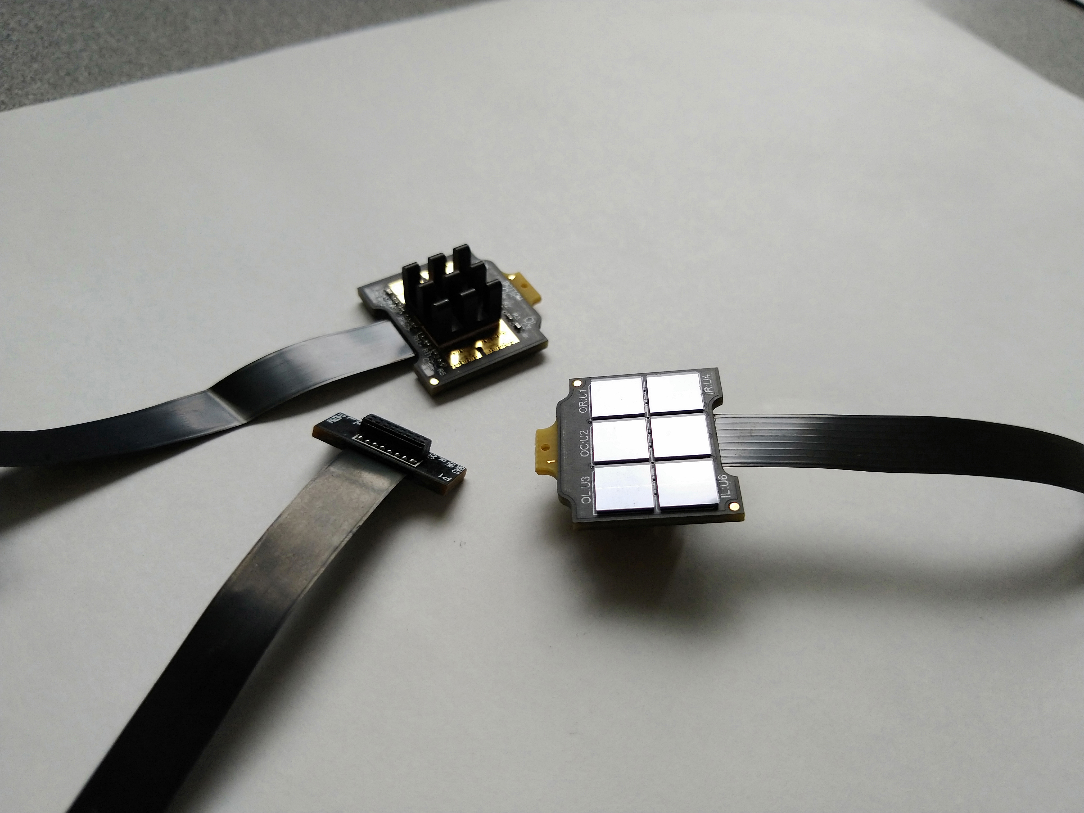
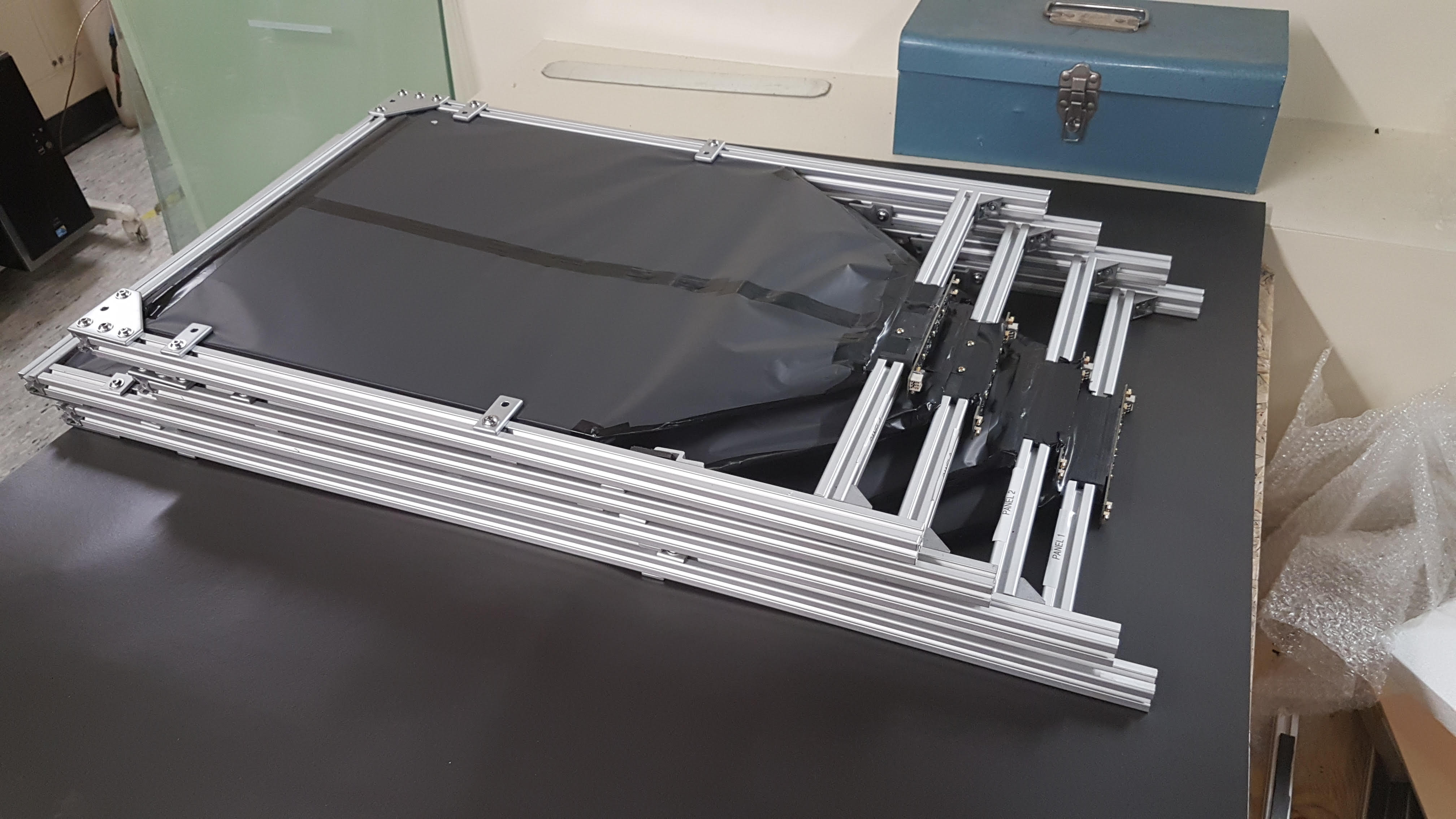
When this avalanche photodiode is operated in the so-called Geiger mode, i.e., the bias voltage is slightly above the breakdown threshold, it has single photon sensitivity. A single SiPM is made of tens of thousands of these photodiodes packed in an area of approximately 1 cm2. The operational voltage of these devices is about 30 V. In ALPHA an array of six SiPMs is coupled to a bundle of fibers that “extracts” the light from the scintillator panel. Given the smallness of the SiPMs, two of such arrays are placed side by side, both looking at the light of a single panel. The time coincidence of the signals produced by the two arrays is sufficient to get rid of the dark noise counts.